

pcb fabrication layout
group namePCB layout
-
Min Order1 piece
brand nameZLONE
modelzlx
payment method
-
update timeThu, 15 Nov 2012 10:20:07 GMT
Paramtents
green red
Packging & Delivery
Min Order1 piece
Briefing
Detailed
We can offer 1 to 12 Layer PCB fabrication, PCB design, PCB layout, PCB manufacturing, PCB Assemblies, components sourcing, PCBA Function Test, design solution.
pcb fabrication layout:
1. PCB gerber file.
2. BOM LIST FOR PCB ASSEMBLY.
3. Send us your sample pcb board or PCBA.
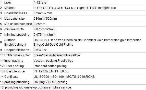
PCB Specification of ZLX technology:
Shenzhen ZLX Technology Co.,Ltd is a leading high technology company,specializing in software design,hardware design ,creative design, industrial design ,structural design and supply chain management of electronic products with one year quality warranty for all customers.
1.With our technicians offering their rich 30-year experience in electronics OEM/ODM with clients,while our QC engineer has more than 10 years experience in foreign-owned enterprises; our sales team has 10 years of experience in exporting with foreign language skills in English, with "To help our customer more successful" as our mission.
2. Location: Shenzhen is the PCB supply chain centre and the biggest Electronic Components Center in Asia. Specially,Shenzhen is near three seaports:1 hour to Yantian,2 hour to Shekou and Zhuhai.
3. We have strong R&D capacity, which can meet to customers’ particular requirements.
4. Certificates: We are an ISO 9001:2008 and IPC registered enterprise, and our products carry TUV ,SGS and RoHS marks.
5. We purchase key components from our partner factories in bulk, ensuring we have the components. Our SMT lines from Yamaha and Siemens ensure the best quality.
6. Our customers locate in North and South America, Europe, Asia, Oceania and Africa. We earn good reputation among clients.


