


FR4 Multilayer PCB Manufacturing With Blue Peelable Mask Layer
group nameMultilayer PCB Manufacturing
-
Min Order1 piece
brand namePCBQuick PCB Manufacturing and Assembly
modelKF-FR4 PCB-52
payment methodL/C, D/A, D/P, Western Union, MoneyGram, T/T, Paypal
-
update timeFri, 30 Jul 2021 13:54:38 GMT
Paramtents
Material FR4
Board Thickness 1.6mm
Soldermask Color Green
Silkscreen Color White
Surface Technics ENIG
Packging & Delivery
Min Order1 piece
Briefing
Can peel blue glue for a single component touch screen insulation protection, insulation, moisture and protection.
Detailed
Blue peelable mask layer is applied to:
1. Corrosion protection of various acid and alkali solutions;
2. Protection against electric corrosion of various electroplating solutions;
3. Various electroless plating protection.
Do not print blue glue under the following circumstances
1, surface treatment for tin, silver and other easy to be oxidized and easy to wipe the board, not printed blue glue.
Reason: this plate surface treatment process is easy to be oxidized, can not bake the plate, but after printing the blue glue must be through the baking plate to solidify the blue glue.
2, not double-sided printing blue glue.Reason:
A) double-sided blue glue enters the hole, and it is difficult to tear off the blue glue;
B) after printing one side, the blue glue bulges, causing uneven, inconvenient printing the other side, and easy to cause plate bending problems;
C) plate bending is not easy to measure.
Peelable mask pcb performance
1. No solvent volatilization, environmental protection and safety, almost 100% solid content, almost the same thickness of dry and wet film;
2. High thixotropy, effectively ensuring smooth screen printing edge, strong cover pore force and slight vertical flow;
3, good adhesion is not peeling off;
4. Easy to peel, complete, no residual flow, no impact on the bottom layer;
5, does not contain any metal and non-metal monomer, corrosion resistance process will not dissolve any material, no impact on the original solution. The pass hole is easy to be peeled off without residue and has no effect on the original solution.
Curing conditions
Required drying conditions |
First printing |
Second printing |
Double-sided printing |
Cabinet oven temperature & time |
150℃ 5min |
150℃ 3-10min |
150℃ 15-20min |
Infrared tunnel furnace temperature & time |
160℃/180℃ 1-1.5min |
160℃/180℃ 2-3min |
160℃/180℃ 2-3min |
Uv curing Energy, speed | 1000-3000J 4-5min | 1000-3000J 3-4min | 1000-3000J 3-4min |
Fr4 multilayer PCB process capability
| NO | Item | Craft Ability | |
| 1 | Surface Finish | HASL,Immersion Gold,Gold Plating,OSP,Immersion Tin,etc | |
| 2 | Layer | 1-30 layers | |
| 3 | Min.Line Width | 3mil | |
| 4 | Min.Line Space | 3mil | |
| 5 | Min.Space between Pad to Pad | 3mil | |
| 6 | Min.Hole Diameter | 0.10mm | |
| 7 | Min.Bonding Pad Diameter | 10mil | |
| 8 | Max.Proportion of Drilling Hole and Board Thickness | 1:12:05 | |
| 9 | Max.Size of Finish Board | 23inch*35inch | |
| 10 | Rang of Finish Board′s Thickness | 0.21-7.0mm | |
| 11 | Min.Thickness of Soldermask | 10um | |
| 12 | Soldermask | Green,Yellow,Black,White,Red,transparent photosensitive solder mask,Strippable solder mask | |
| 13 | Min.Linewidth of Idents | 4mil | |
| 14 | Min.Height of Idents | 25mil | |
| 15 | Color of Silk-screen | White,Yellow,Black | |
| 16 | Date File Format | Gerber file and Drilling file,Report series,PADS 2000 series,powerpcb series,ODB++ | |
| 17 | E-testing | 100%E-Test:High Voltage Testing | |
| 18 | Material for PCB | High TG Material:High Frequence(ROGERS,TEFLON,TADONIC,ARLON):Haloger free Material | |
| 19 | Other Test | Impedance Testing,Resisitance Testing,Microsection etc | |
| 20 | Special Technological Requirement | Blind&Buried Vias and High Thickness Copper | |
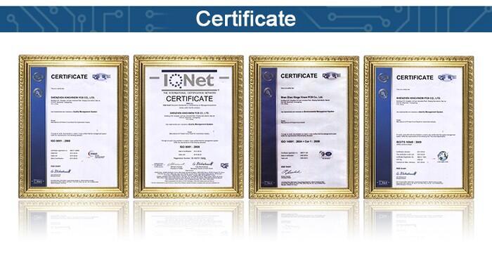
PCBQUICK PCB Certificates
UL, TS16949, ISO14001, ISO9001-2008, and RoHS
You need a product


You May Like


- Nearest port for product export
- SZ
- Delivery clauses under the trade mode
- FOB, EXW, DDU, Express Delivery
- Acceptable payment methods
- T/T, PayPal, Westem Union, Cash, Escrow
- Export mode
- Export through agents