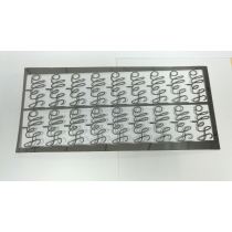
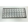
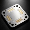
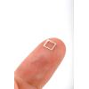
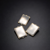
One-step forming of fine slits and micropores
Etching minimum line width/gap can be 0.02 - 0.05 mm, dense array and profile is not limited by the mold.
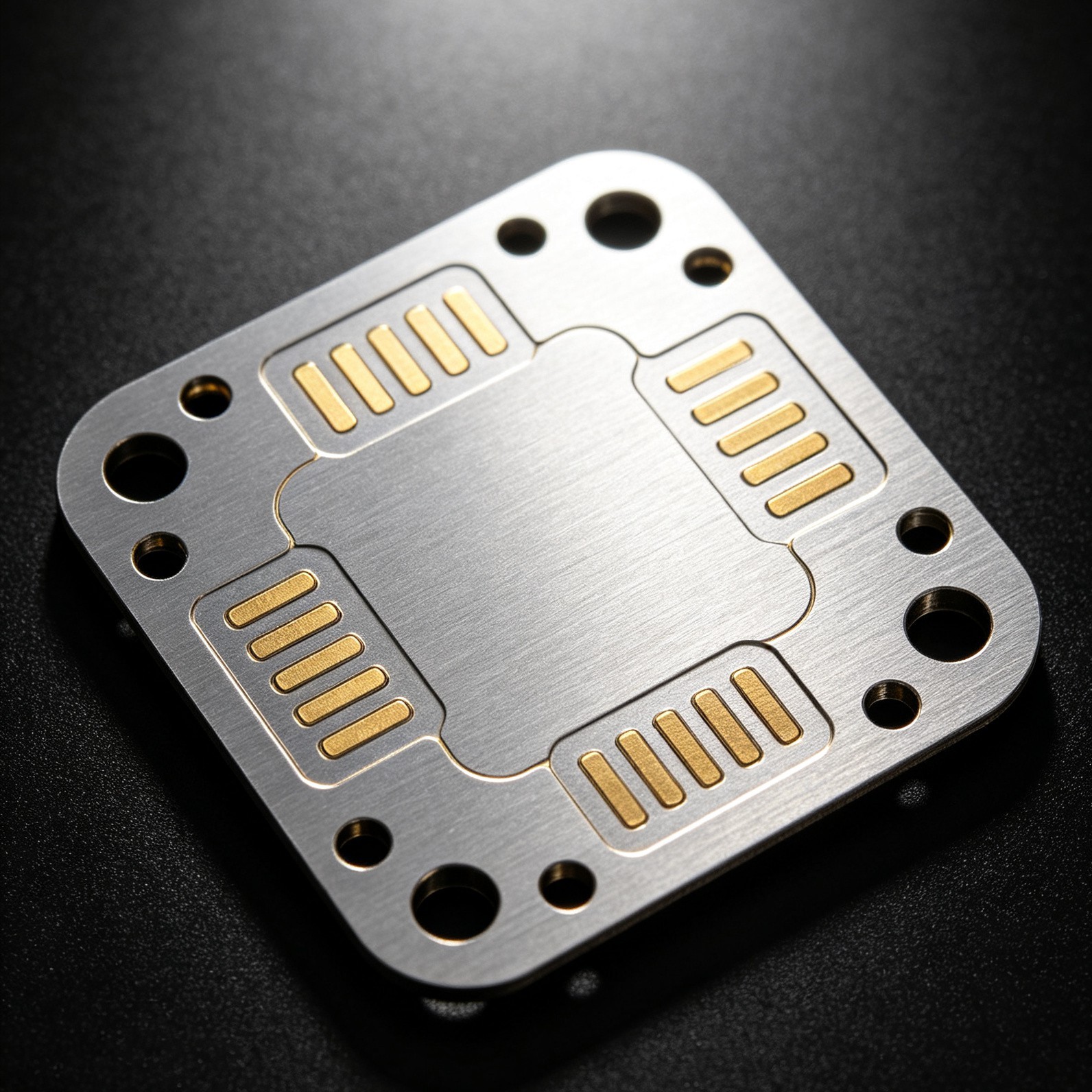

group nameSemiconductor
Min Order1 piece
brand nameMicroEtch
payment methodT/T, L/C, PayPal, Westem Union
update timeTue, 27 Oct 2026 05:50:49 GMT
Material nickel silver (C7701), SUS304 / SUS301 stainless steel…
Specifications 0 mould fee | 0.02 mm | 24 hours; etching tolerance ±0.01 mm…
Function Elastic contacts formed in one etching pass with stable contact resistance and long insertion life
Application RF and communication device makers / Consumer and automotive electronics / Semiconductor packagers
Industries Electronics / communication / automotive / semiconductor industry
Business Model OEM / ODM custom manufacturing from drawings; sample to volume production
Business Type OEM / ODM Manufacturer
Min Order1 piece
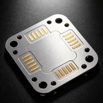
Etched Transistor Socket Contact / Socket Part for OEM / ODM Programs Transistor Socket Contact / Socket Part is a precision metal part with micro-apertures, fine slots or custom geometry formed directly into nickel silver (C7701), SUS304 / SUS301 stainless steel, beryllium copper — selected by shielding and spring requirements by photo-chemical etching — integrally formed and tooling-free. Its purpose is straightforward: elastic contacts formed in one etching pass with stable contact resistance and long insertion life. What is it? Elastic contacts formed in one etching pass with stable contact resistance and long insertion life Typical uses: RF and communication device makers / Consumer and automotive electronics / Semiconductor packagers Why specify etched Transistor Socket Contact / Socket Part Etching minimum line width/gap can be 0.02 - 0.05 mm, dense array and profile is not limited by the mold. Non-contact chemical cold working, no stamping shear and collapse edge, avoid short circuit, scratch and poor contact. Etching first, bending, pressing, half shearing, shielding cavity and buckle can be completed on the same part at one time. Product specification Send us the machine model and shielding position, outline, cavity height and assembly method, shielding effectiveness target, plating and soldering requirements. We will recommend material, geometry and process, and issue a sample for validation. Built around B2B buying paths fine slots, micro-holes and custom cavities etched in one pass, samples within 24 hours. etching combined with pressing for bent, dimpled and clipped parts, no outsourcing. Kovar, nickel silver and beryllium copper processed to hermeticity and plating requirements. Send your drawing and requirement Send us the machine model and shielding position, outline, cavity height and assembly method, shielding effectiveness target, plating and soldering requirements. We will recommend material, geometry and process, and issue a sample for validation. Start with the material grade, thickness and tolerance your application requires. Buyer FAQ 0.05 mm typical, down to 0.02 mm at the limit, depending on material thickness. Parts are etched first and then pressed, so bends, dimples, half-shears and clips are all produced in one flow. Yes. Kovar, beryllium copper, nickel silver and SUS301 are all in regular production; sample first to validate. Tin or nickel for solderable areas; gold for contact and conduction surfaces — tailored to salt-spray and contact-resistance requirements.
Etched Transistor Socket Contact / Socket Part — Custom / Socket Part
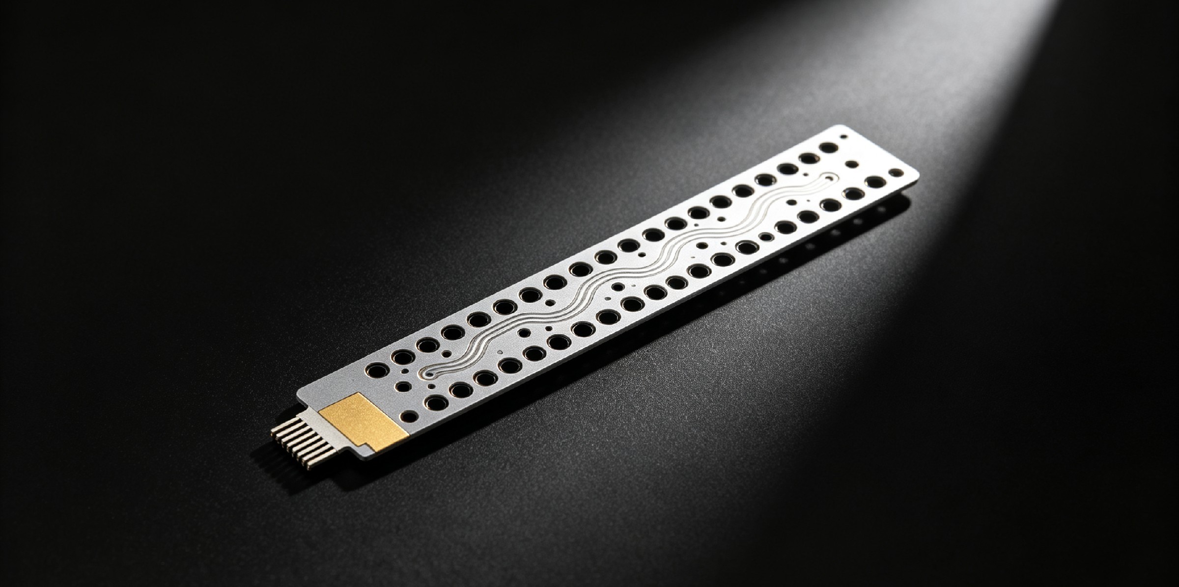 0 mould feeOptical film — revisions need no tooling
24 hoursSample turnaround
±0.01 mmnickel silver (C7701), SUS304 / SUS301 stainless steel…
Turn Your Transistor Socket Contact / Socket Part Requirement into a Manufacturable Part
One-step forming of fine slits and micropores
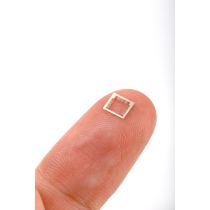
Side wall vertical without burrs
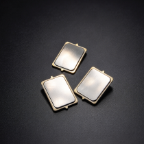
Etching + stamping composite
Core Details for Sourcing Review
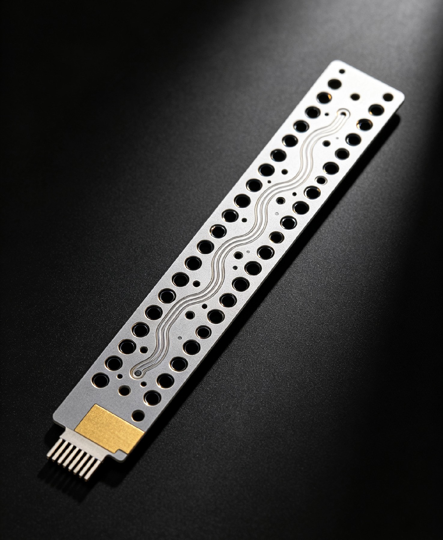
Product type Etched Transistor Socket Contact / Socket Part Materials nickel silver (C7701), SUS304 / SUS301 stainless steel… Process Photo-chemical etching, integrally formed Specifications 0 mould fee | 0.02 mm | 24 hours; etching tolerance ±0.01 mm… Function Elastic contacts formed in one etching pass with stable contact resistance and long insertion life Applications RF and communication device makers / Consumer and automotive electronics / Semiconductor packagers Industries served Electronics / communication / automotive / semiconductor industry Business model OEM / ODM custom manufacturing from drawings; sample to volume production Tooling Optical film based — no mould fee for design revisions Sampling Sample issued within 24 hours. 5–15 days for volume production
Support for OEM, Brand and Distribution Programs
RF and communication device makers
Consumer and automotive electronics
Semiconductor packagers
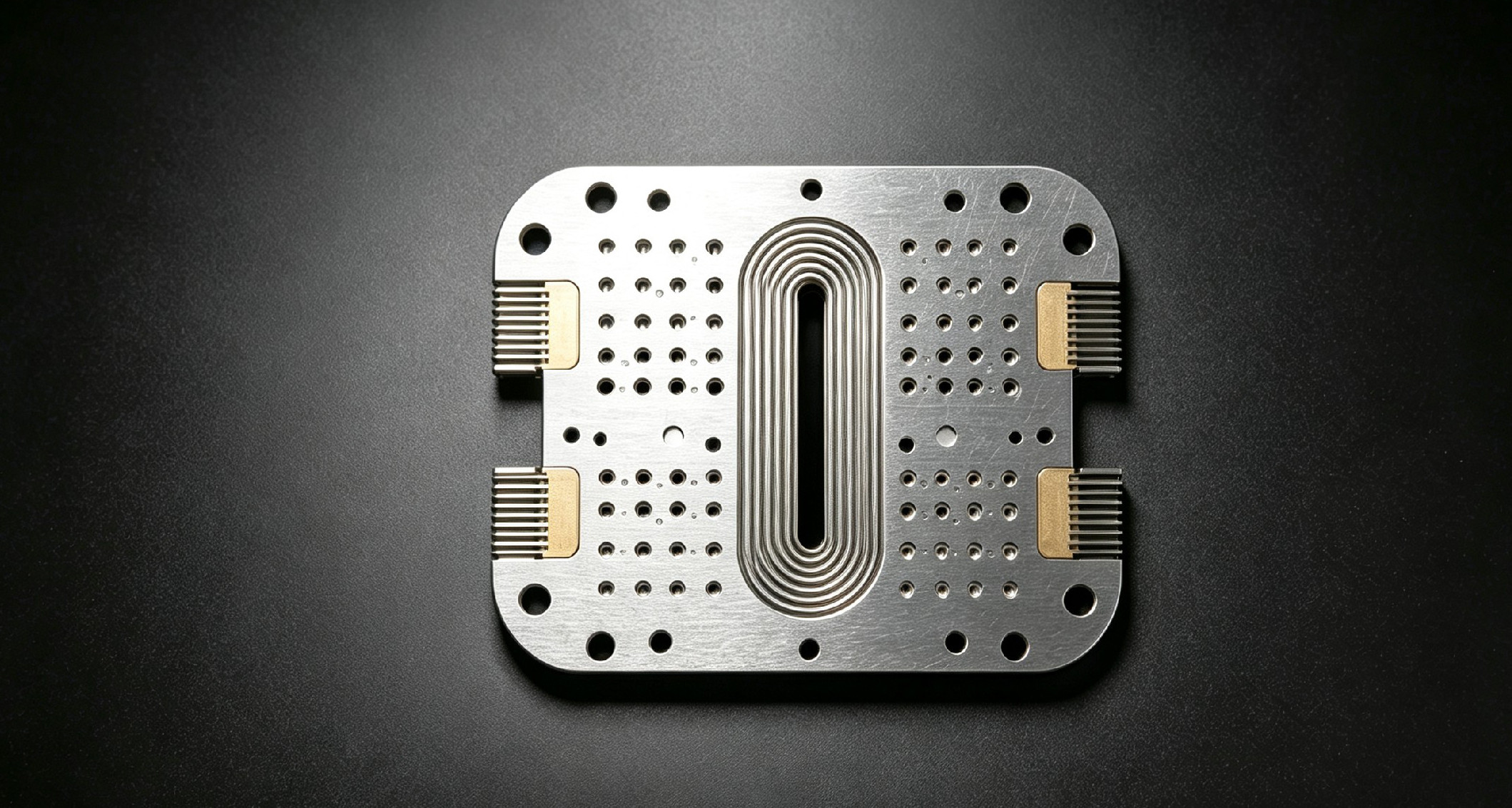
Get Transistor Socket Contact / Socket Part Samples in 24 Hours
Questions Buyers Ask Before Enquiry
How fine can slots and hole arrays be?
What about bends and clips?
Can you process Kovar or beryllium copper?
Which plating should we choose?
6YRS Ji'an Zhuanjing Technology Co. Ltd.
网络文化经营许可证:浙ICP备14006100号-11 2007-2026 Tradevv.com. All rights reserved.