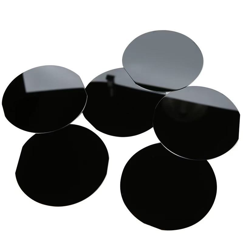


Custom Monocrystalline Silicon Wafer, 1–12 Inch Single Crystal Si Wafer For Semiconductor
group nameLaser Focus Lenses
-
Min Order1 piece
brand nameFELIX GLASS optical glass Manufacturing base
modelFG-MONO-SI-WAFER
payment methodL/C, D/A, D/P, Western Union, MoneyGram, T/T
-
update timeTue, 08 Sep 2026 18:11:02 GMT
Paramtents
Substrate Material High purity monocrystalline silicon (CZ / MCZ / FZ growth)
Size Range Custom diameter 1", 2", 3", 4", 5", 6", 8", 12" (25.4mm–300mm)
Customizable Spec Orientation <100>/<111>/<110>, N/P type, resistivity, single/double side polished
Core Application Semiconductor IC, MEMS, lab material test, optical infrared substrate, solar cell substrate
Packging & Delivery
Min Order1 piece
Briefing
Custom high-purity monocrystalline silicon wafer covering 1–12 inch sizes, customizable crystal orientation, conductive type
Detailed
Custom Monocrystalline Silicon Wafer, 1–12 Inch Single Crystal Si Substrate
Felix Glass monocrystalline silicon wafer is manufactured by CZ, MCZ or FZ single crystal growth technology, available in full sizes from 1 inch to 12 inch, fully customizable crystal orientation, doping type, resistivity, thickness and surface polishing process.
Silicon wafer owns excellent semiconductor electrical properties, stable thermal conductivity and outstanding infrared transmission performance, serving as core substrate for semiconductor chip manufacturing, MEMS devices, laboratory material analysis, infrared optical windows and photovoltaic cells. We supply single-side polished, double-side polished, etched, ground silicon wafers, support thermal oxide layer deposition, metal coating OEM customization.
Core Optical & Electrical Specifications
- Raw Material: High purity monocrystalline silicon (99.9999999% purity)
- Standard Sizes: 1", 2", 3", 4", 5", 6", 8", 12" (25.4mm~300mm)
- Crystal Orientation: <100>, <111>, <110>, custom offset angle optional
- Conductive Type: N-type, P-type, intrinsic semi-insulating silicon
- Resistivity Range: 0.001~20000 Ω·cm customizable
- Surface Treatment: Single side polished (SSP), double side polished (DSP), grinding, etching
- Thickness Range: 25μm ultra-thin ~ 1200μm thick wafer
- Surface Quality: TTV<10μm, low particle, low dislocation density, semiconductor prime grade
All standard specs can be adjusted to meet your unique semiconductor lab & production requirements.
Core Product Advantages
1. Full size coverage 1–12 inch, support non-standard special diameter customization
2. Multiple crystal orientation & conductive type options, match different semiconductor device demands
3. Ultra-high purity monocrystalline ingot, low impurity, stable electrical performance for long-term chip production
4. Multiple surface polishing & processing solutions, can add thermal oxide, metal film coating as OEM demand
5. Flat ultra-smooth polished surface, low surface defect, ideal substrate for SEM, AFM, laser spectral testing
6. Factory direct supply, small lab sample order & mass semiconductor production order both acceptable
Typical Application Scenarios
- Semiconductor IC, diode, transistor, photodetector manufacturing substrate
- MEMS micro-electromechanical system, sensor chip production base
- Laboratory SEM, AFM, Raman, FTIR material characterization test substrate
- Infrared optical window, silicon-based photonic integrated circuit platform
- Solar cell, photovoltaic power device substrate
- Micro-nano film deposition, PVD/CVD epitaxial growth carrier
OEM Manufacturing Capability
We provide full one-stop monocrystalline silicon wafer processing including single crystal ingot slicing, lapping, etching, double-side ultra-precision polishing, thermal oxidation, metal coating, clean room packaging. Small sample trial, batch mass customization and long-term factory supply are supported. Every silicon wafer passes full electrical resistivity, surface flatness and particle inspection before delivery.
Standard FAQ
1. What size monocrystalline silicon wafers can you customize?
We support full standard sizes from 1 inch to 12 inch, also accept non-standard special diameter customized silicon wafers.
2. What is the difference between N-type and P-type silicon wafer?
N-type doped with phosphorus for electron conduction; P-type doped with boron for hole conduction, selected according to customer semiconductor device design.
3. Can I customize oxide layer and metal coating on silicon wafer surface?
Yes, we provide thermal dry/wet oxide growth, gold, chrome, titanium metal coating OEM service with customizable film thickness.
4. What lab equipment uses silicon wafer as test substrate?
Silicon wafer is widely used for SEM, AFM, Raman spectroscopy, FTIR infrared spectrum, thin film deposition experimental substrate.
5. Do you support small quantity lab sample orders?
We accept 1 piece small lab sample orders, provide full technical parameter test report for each batch silicon wafer.
Related Products:
Plano Convex Spherical Lens,
AR Coated Optical Window,
Laser Line Filter,
Custom Optical Prism
Optical Domes
Infrared Optical Components
You need a product
You May Like
- Nearest port for product export
- Shenzhen, Guangzhou
- Delivery clauses under the trade mode
- FOB, CFR, CIF, EXW, FAS, CIP, FCA, CPT, DEQ, DDP, DDU, Express Delivery, DAF, DES
- Acceptable payment methods
- T/T, L/C, D/P D/A, MoneyGram, Credit Card, PayPal, Westem Union, Cash, Escrow